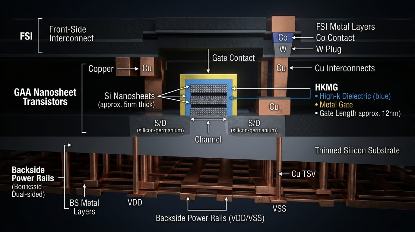
On September 9, 2026, Taiwan Semiconductor Manufacturing Company (TSMC) confirmed that its enhanced 2-nanometer process node, designated N2P, has successfully passed crucial defect-density and yield qualification gates at its Hsinchu Fab 20 research facility, meeting commercial thresholds several months ahead of internal engineering projections.
N2P marks TSMC's most consequential structural semiconductor innovation in more than a decade. While the baseline N2 node introduced gate-all-around (GAA) nanosheet transistors—replacing the FinFET architecture that powered the semiconductor industry from 22nm down to 3nm—N2P introduces Super Power Rail (SPR), TSMC's proprietary implementation of Backside Power Delivery Network (BSPDN) technology.
In conventional front-side power delivery, both power supply lines (VDD, VSS) and signal interconnects are fabricated above the transistor layer across 15 to 20 increasingly dense metal layers. As feature sizes shrunk into single-digit nanometers, wire resistance escalated exponentially, causing severe resistance-capacitance (RC) latency bottlenecks and parasitic voltage loss (known as IR drop). Transistors were starved of clean voltage, generating parasitic heat and wasting up to a quarter of total dissipated energy.
TSMC's Super Power Rail physically decouples these functions. Power rails and large power via contacts are relocated entirely to the backside of a thinned silicon wafer, connecting directly to the source and drain terminals of the nanosheet transistors through through-silicon vias (TSVs). This eliminates IR drop, enhances power stability under extreme transient current spikes, and frees up the entire front side of the die for relaxed, low-resistance signal routing.
The empirical gains are striking. TSMC's validation telemetry demonstrates a 16% reduction in power consumption at identical operating frequencies, or a 10% to 12% boost in clock speed at equal power compared to first-generation N2. For hyperscale AI accelerator designs operating in the 800W to 1,200W thermal envelope, N2P provides essential silicon efficiency to sustain scaling into the multi-trillion parameter era.