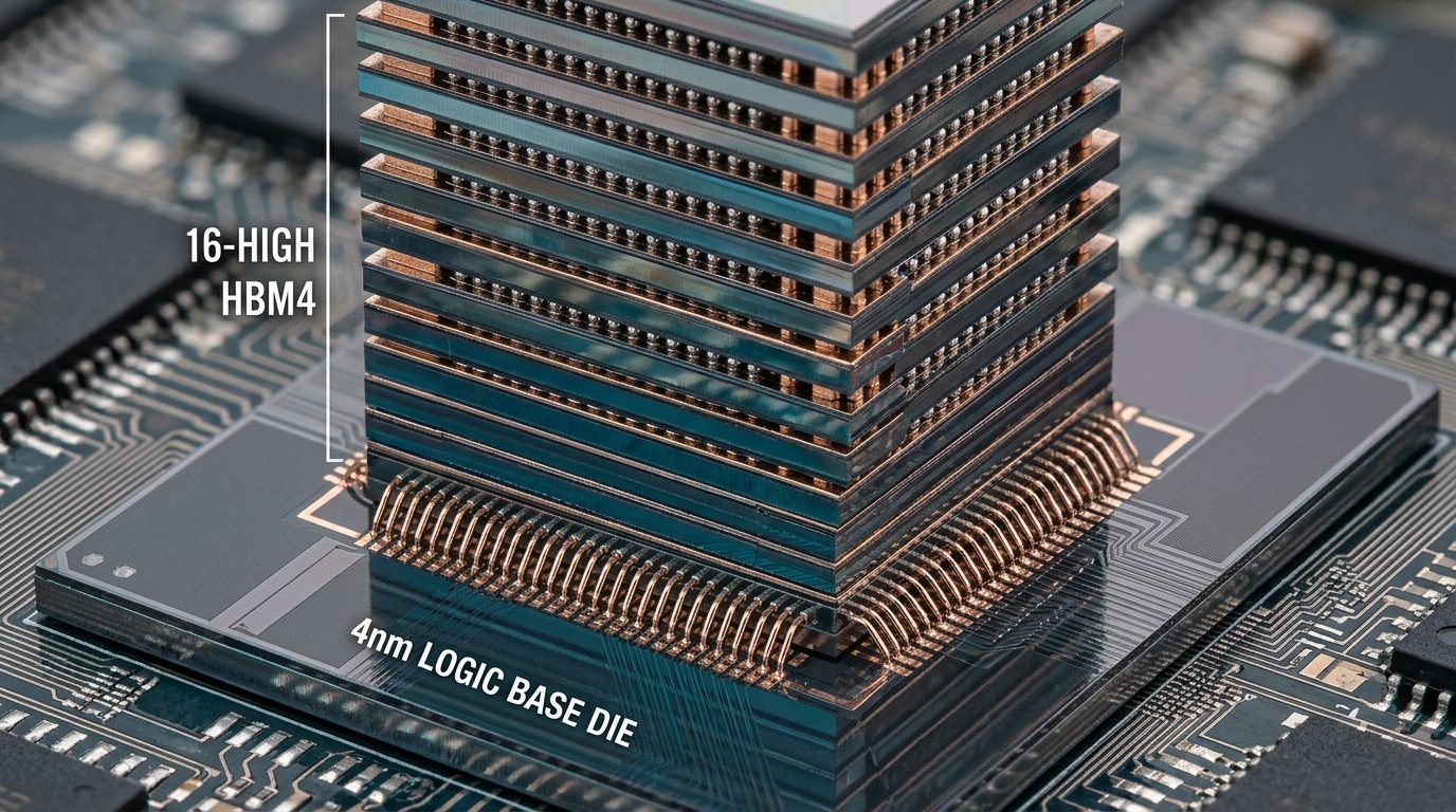
In a major milestone for semiconductor packaging, South Korea's premier memory manufacturers, SK hynix and Samsung Electronics, have achieved working silicon validation for 16-high HBM4 memory stacks. The breakthroughs demonstrate functional 64GB monolithic cubes that smash existing bandwidth and thermal barriers.
Since the advent of generative AI clusters, High Bandwidth Memory has been the lifeblood of accelerated compute. Yet the existing HBM3E standard, limited to 12-high stacks and a 1,024-bit bus width, has pushed conventional packaging physics to its absolute limit. With parasitic capacitance rising and thermal hotspots throttling GPU performance under continuous inferencing workloads, the industry recognized that standard micro-bump soldering could not survive another generation.
HBM4 fundamentally re-engineers the memory stack. Rather than using passive silicon base dies, both manufacturers transitioned to active custom 4nm logic dies. SK hynix partnered with TSMC to fabricate its base die on the N4P node, while Samsung leveraged its proprietary 4nm Gate-All-Around (GAA) process. By embedding logic circuits directly underneath the 16 DRAM layers, the base die handles high-speed signal routing, built-in self-test (BIST), and even localized near-memory data decompression.
The physical integration of 16 individual DRAM dies within the JEDEC-mandated package height constraint of 720 micrometers required the abandonment of micro-bump interconnects. Both companies deployed direct copper-to-copper (Cu-Cu) hybrid bonding. By polishing wafer surfaces to atomic smoothness and bonding copper pads directly without solder, the vertical interconnect pitch is reduced from 25 microns to less than 3 microns, yielding a 33% improvement in thermal dissipation.
The resulting performance metrics are staggering. Each 16-high HBM4 cube provides 64GB of capacity and operates at memory speeds of up to 3.2 Terabytes per second. When integrated into an AI accelerator housing an eight-cube memory ring, total system memory reaches 512GB with an aggregate memory bandwidth surpassing 24 Terabytes per seconda 300% bandwidth leap over current H200 and B200 systems.
As hyperscalers prepare for 2027 datacenter deployments, the silicon validation of 16-high HBM4 confirms that the physical memory wall is being held at bay, providing the prerequisite hardware platform for the next leap in trillion-parameter autonomous foundation models.