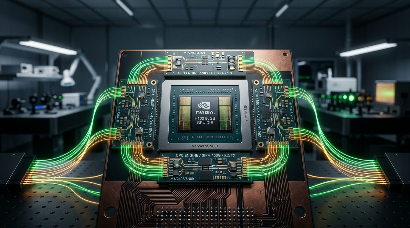
In a decisive technical milestone for high-performance computing infrastructure, NVIDIA, TSMC, and Broadcom have announced the tape-out and functional silicon validation of production-ready 1.6 Terabit-per-second Co-Packaged Optics (CPO) engines.
For the past three decades, datacenter networks have relied on pluggable optical transceivers mounted on the faceplates of top-of-rack switches. Electrical signals generated by GPU computing dies had to travel several inches across organic printed circuit boards (PCBs), through ball grid array (BGA) sockets, and along copper traces before reaching an optical transceiver module to be converted into laser light. At historical speeds of 10 or 25 Gigabits per second, the electrical losses along this path were manageable.
However, as modern AI clusters transitioned to 112 Gbps and 224 Gbps SerDes signaling to feed ravenous transformer training workloads, electrical copper encountered insurmountable physics. At 224 Gbps, high-frequency signals attenuate exponentially over just a few inches of copper, forcing designers to install power-hungry signal retimer chips every few centimeters. In modern 100,000-accelerator datacenters, simply shuttling bits across circuit boards accounts for nearly a third of all electrical consumption.
Co-Packaged Optics solves this by relocating the optical engine onto the accelerator substrate itself. Leveraging TSMC's Compact Universal Photonic Engine (COUPE) technology, an electronic driver integrated circuit (EIC) is stacked directly on top of a silicon photonics integrated circuit (PIC) using sub-micron 3D bonding. This compact optical engine sits less than 15 millimeters from the main GPU compute die, connected via short, ultra-low-capacitance traces.
Laser light is fed into the package through miniature glass optical fibers attached directly to the silicon photonics die. In laboratory characterizations, the 1.6T CPO engine achieved aggregate data throughput of 1.6 Terabits per second while consuming only 3.4 picojoules per bit—a 72% reduction compared to standard pluggable optical links. Furthermore, latency across the host-to-fiber interface dropped by 45 nanoseconds per hop.
With hyperscalers facing severe regional electrical grid constraints, the transition from electrical copper to co-packaged optical silicon represents the defining physical hardware transition enabling trillion-parameter AI training clusters for the decade ahead.