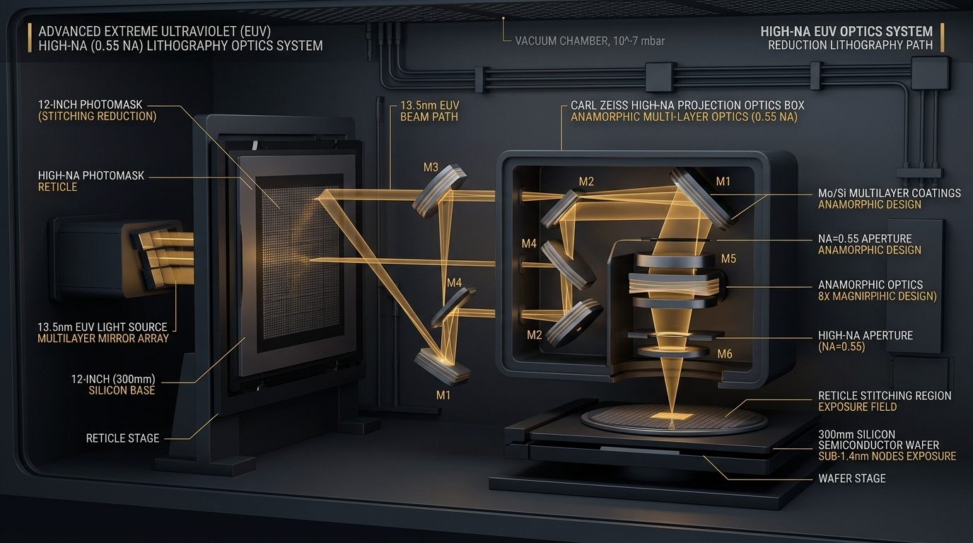
In a dual landmark announcement for global semiconductor manufacturing, ASML and lead customer Intel Foundry confirmed that more than one million production wafers have now been successfully patterned on High-NA Extreme Ultraviolet (EUV) lithography scanners. Simultanously, ASML unveiled the formation of the 12-Inch Photomask Consortium, uniting Intel, TSMC, and Samsung Electronics to modernize the physical foundations of optical lithography.
The commercialization of High-NA EUV, which increases the numerical aperture from 0.33 to 0.55 using 13.5nm wavelength light, has been the critical enabler for sub-2nm transistor scaling. However, High-NA introduced a major geometric compromise: anamorphic magnification. Because Carl Zeiss optical mirrors could not support 8x reduction across both axes without causing EUV light to strike the photomask at excessively steep angles (causing shadowing), High-NA adopted 4x reduction in the scan direction and 8x reduction in the slit direction.
This anamorphic design cut the maximum printable exposure area on the wafer from the traditional 26mm × 33mm (858 mm²) down to a half-field of 26mm × 16.5mm (429 mm²). For small smartphone application processors, half-field exposures are manageable. But for frontier artificial intelligence accelerators—such as NVIDIA's Blackwell (which spans two 858 mm² reticle-limit dies) and Cerebras wafer-scale components—chips exceed the 429 mm² boundary. Foundries were forced to utilize 'reticle stitching,' exposing two halves of a single die sequentially. Stitching slashes scanner throughput by roughly 40%, increases machine cycle time, and introduces edge-placement overlay errors at the stitch boundary.
To permanently eliminate the stitching bottleneck, ASML's 12-Inch Photomask Consortium proposes replacing the 50-year-old 6-inch × 6-inch (152mm × 152mm) quartz plate standard with 12-inch (300mm) circular silicon-substrate photomasks. By doubling the mask area, an anamorphic High-NA scanner can project a full 26mm × 33mm field in a single continuous scan.
Transitioning the entire supply chain—including mask blank deposition by Hoya and AGC, multi-beam mask writing by IMS Nanofabrication, actinic EUV inspection by KLA, and robotic pod handling—will require an estimated $8 billion in collective industry investment. ASML projected that initial pilot lines for 12-inch masks will be operational by 2031, with high-volume foundry manufacturing timed for 2033 to support Hyper-NA (0.75 NA) and sub-1nm logic nodes.