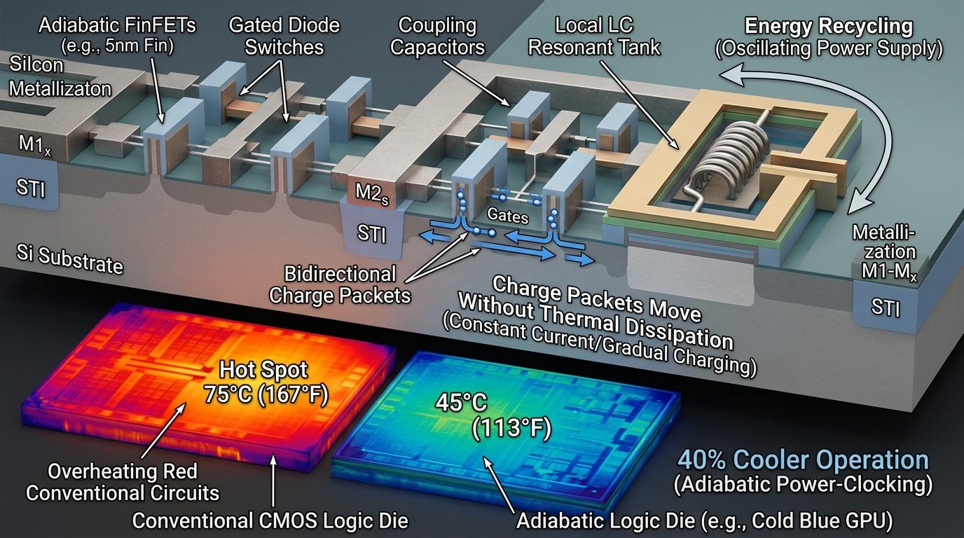
In a landmark technical paper spotlighted by MIT Technology Review on September 8, 2026, researchers demonstrated a practical resolution to the semiconductor industry’s most pressing physical crisis: waste heat dissipation.
In standard CMOS digital logic, whenever a transistor flips from 0 to 1, charge flows from the power rail into the gate capacitor. When it flips back to 0, that stored electrostatic charge is dumped straight to ground through resistance, converting high-grade electrical power directly into waste thermal heat (governed by the fundamental formula P = αCV²f). At billions of cycles per second across tens of billions of transistors, this creates immense thermal concentrations.
Adiabatic computing circumvents this thermodynamic penalty by replacing rigid DC voltage supplies with multi-phase AC resonant power clocks. By ramping the voltage gradually, charge transfers onto the gate capacitance without crossing a large voltage drop, eliminating resistive switching loss. When the computation cycle completes, the resonant inductive clock draws the stored charge back out of the transistor and recycles it into the power supply reservoir for the next clock phase.
Previous attempts at adiabatic logic suffered from severe clock frequency penalties. However, by combining high-Q on-chip magnetic inductors with GaN-on-silicon power stages, the research team achieved switching speeds exceeding 2.5 GHz while maintaining over 70% charge recovery efficiency.
For AI hyperscalers grappling with exorbitant cooling infrastructure and constrained power utility feeds, adiabatic circuit design represents the most consequential architectural pivot since the transition from bipolar junction transistors to CMOS forty years ago.